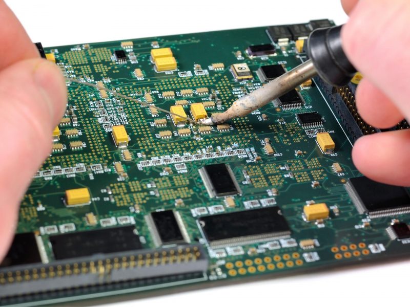
With components becoming smaller and more compact, the chances of soldering issues occurring have become higher. Especially, if your PCB is going to be used for an important application, it will be more important than ever to know what a good solder joint looks like.
Here’s a guide to help you discern what’s good and what’s not, so that you may be sure to avoid these soldering issues for your projects, or just to be able to do a quality assessment on assembled PCBs received from a third party.
Ideal Solder Joints
When looking for solder defects, it’s helpful to have an image of an ideal solder joint for comparison.
The ideal solder joint for through-hole components is a “concave fillet”, which has a smooth and shiny concave surface at an angle of 40 to 70 degrees from the horizontal, which looks just like the shape of a Hershey’s kiss. It can be achieved when the soldering iron is at the right temperature, with the oxide layer cleaned from the PCB contacts.
The Ideal Surface Mount Solder Joint
Similarly, good SMD solder joints have smooth, concave fillets as well.
Hence, the general characteristics of a good solder joint:
– Has good and complete wetting
– Has a concave fillet
– Is shiny and clean
Bad Solder Joints
Unfortunately, there are many ways for solder joints to go wrong, as solder always seems to go where it isn’t supposed to.
1.Solder Bridging
Of the many problems caused by smaller and smaller components, solder bridging takes the top of the list. It forms when two or more solder joints become inadvertently connected, usually due to the excessive application of solder between joints or using soldering tips that are too big or too wide. Identifying a solder bridge can sometimes be challenging, as solder bridges can be microscopic in size. If left undetected, it can lead to a short circuit and cause a component to burn up.
A solder bridge can be fixed by holding your solder iron in the middle of the bridge to melt the solder, and drawing it through to break the bridge. If the solder bridge is too large, excess solder can be removed a solder sucker.
2.Excessive Solder
If you get too enthusiastic and apply too much solder onto a pin, excess buildup is what you’ll get, characterized by its rounded shape. A common beginner’s assumption is the more solder the better but while more solder should increase the amount of material forming the joint, it is difficult to know what actually happened beneath that mass of solder. There still lies a possibility that neither the pin nor the pad is properly wetted. It also increases the risk of solder bridges forming so it’s better to be safe than sorry. Enough solder to adequately wet the pin and the pads thoroughly is usually sufficient and the concave surface remains the best shape to have as it allows us to better access the wetting of the joint.
3.Solder Balling
Solder balls are also one of the most common soldering defects that occur typically with wave or reflow soldering. It appears as a small sphere of solder that adheres itself to a laminate, resist, or conductor surface. Solder balls can be a result of several factors, such as improper solder paste printing, poor reflow temperature settings, rough PCB design, or the usage of oxidized electronics components.
4.Cold Joint
The surface of cold joints appears dull, lumpy and pock-marked. This is typically caused by insufficient heat being transferred to the joint to completely melt it which may be a result of a number of different things. The solder iron or the joint itself may not have been given enough time to heat up sufficiently, the iron temperature may not be set high enough to melt the particular solder type being used (e.g. lead-free solder has a higher melting temperature) or, it may be a result of the design of the pads and traces themselves. For example, a pad connected directly to the ground plane without thermal relief considerations will cause the heat of the solder iron to be lost to the ground plane. If you find a stubborn solder joint that refuses to liquify then the design may be at fault. If not properly rectified, cracks will be more likely to form over time, leading to eventual failure.
5.Overheated Joint
Just as too little heat will cause wonky joints, too much heat will also give you a splitting headache. Overheated solder joints can result from the soldering iron temperature being set too high, or result from solder failing to flow, possibly due to the surface of the pad or lead already having a layer of oxide, preventing sufficient heat transfer and therefore leaving you heating the joint for too long. Hopefully, the damage caused will not be severe but it may cause pads to lift entirely, killing the board or requiring costly repairs. Avoid this by choosing the correct solder iron temperature and use flux to clean dirty looking joints and pads.
6.Insufficient Wetting (Through-hole)
Joints that are not fully wetted are weak and do not form a strong connection with the board. Ideally, the solder should achieve 100% wetting with the pad and pin, leaving no gaps or spaces exposed. Insufficient wetting of the pin and pad result in the inability to apply heat to the pin and pad, and insufficient time to flow. Sometimes, it could just be due to a dirty board. The technique to repair this is to clean the board thoroughly and evenly heat both the pad and the pin.
7.Insufficient Wetting (Surface Mount)
Similarly, SMD components can also suffer from insufficient wetting. In the image above, 3 pins of an SMD component do not have good wetting with their respective pads. The solder on the pins had failed to flow onto the pads, as the pin was heated instead of the pad. The solution to repairing this defect is to heat the solder pad with the tip of your soldering iron, then applying more solder until it flows and melts together with the solder already on the pin.
8.Solder Skips
A solder joint that is not wetted with solder is generally referred to as a solder skip. It occurs when solder skips over a surface mount pad, resulting in an open circuit. The cause of solder skips can be a combination of slip-ups in the design or during manufacturing. You may have placed down an uneven pad size, or your manufacturer could have used an incorrect wave height between your board and the soldering wave.
9.Lifted pads
A lifted pad is a solder pad that has become detached from the surface of the PCB possibly due to excessive force on an existing joint or excess heat. Such pads are difficult to work with since the pad is very fragile and can easily tear from the trace. Every effort should be made to adhere the pad back onto the board before attempting to solder to it.
10.Solder Starved
As its name suggests, a solder-starved joint does not have enough solder to form a solid electrical connection. Here, it is likely that insufficient heat was applied to the lead, resulting in a poor connection. It is possible that this joint will work as there is still electrical contact made. Nevertheless, a solder-starved joint is likely to fail eventually as cracks develop over time and weaken the joint. Fortunately, rescuing a solder-starved joint is not difficult. Simply reheat the joint and add more solder.
11.Solder Splashes/Webbing
These bits of solder stick onto the solder mask in untidy splatters, giving the appearance of a spider’s web. These irregularly shaped threads are caused by insufficient use of a fluxing agent or the existence of pollutants on the surface of the boards during wave soldering, and they threaten to cause shorts.
12.Pin Holes and Blow holes
Pin holes and blow hole defects can be easily recognized as they appear as a hole in a solder joint. The terms pin or blow hole will give a clue to the size of the hole, with pin referring to small holes and blow holes being much larger holes. Rather than being a result of bad hand soldering skills, pin and blow holes are usually formed during the wave soldering process. Moisture within the boards is heated into gas during the soldering operation, and escape through the solder when it is still in a molten state. Voids are formed when the gas continues to escape when the solder joint solidifies. Some ways that are employed to avoid this problem is by baking or preheating the boards to take the moisture out, and having a minimum copper plating thickness of about 25um in the through-holes.
What can you do to avoid soldering problems?
While there is no foolproof method to completely prevent soldering problems, there are some good habits we can adopt during PCB design and soldering to reduce the risk of running into soldering issues.
1. Consider solder mask design
Typically green in color, the solder mask the thin polymer coating applied to the surface of PCBs to protect the copper from the environment. Besides preventing oxidation, they also function to prevent solder bridges from forming as well, as solder does not adhere well to the coating. Hence, solder mask can be designed between pads to form a solder mask dam. This is especially helpful for ICs and BGAs where the gap between pads can be as small as a few thousandths of an inch.
2. Place Fiducial marks
Fiducial marks are round solder mask openings with a round bare copper in its center, that are placed on your PCB board during the PCB design stage. There are panel fiducial marks and individual component fiducial marks for components requiring special treatment. Pick-and-Place machines see them as reference points on the PCB to align SMD components on your board during assembly. When used correctly, placement accuracy can be improved. Similarly, if fiducial marks are poorly designed (e.g. poor placement or not enough fiducials), they can lead to poor orientation, increasing the risk of soldering issues.
3. Cleaning and Tinning the tip of your solder iron
Any contaminants or oxidation on the tip would decrease the solder iron’s ability to conduct heat, which in turn would reduce the quality of your solder joints. Hence, it is important to care of your solder tips. Before you start soldering, remember to clean the tip of your iron by rubbing it against a cleaning pad. If your soldering tip is already badly oxidized, you can use a tip activator to rescue it. Simply dip it into the paste-like substance, move it around and let the abrasives do their work, and the surface will be shiny again.
After that’s done, the tip of your iron should also be tinned. Tinning the tip of your iron means to coat the tip with a layer of solder to protect the tip from oxidation and to improve its ability to conduct heat. Clean and tin your solder iron tip after every two or three joints soldered, and another one time at the end of each soldering session. Doing so would extend the life of your soldering iron and improve the quality of your solder joints!