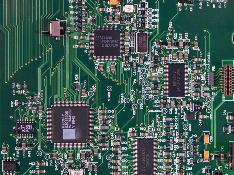
Printed circuit boards (PCBs) play a crucial role in the functioning of electronic devices. These boards are responsible for connecting and controlling various components within a device. Despite their importance, one of the most common problems faced in PCB design is the issue of short-circuits. A short-circuit occurs when two electrical components on the PCB touch each other, causing a direct current flow. This can cause permanent damage to the board and its components and result in the device becoming inoperable. To prevent short-circuits, it is crucial to follow good design practices and implement effective solutions.
Here are some ways to improve the PCB short-circuit issue:
Use of appropriate trace width: Trace width refers to the width of the metal lines on the PCB. It is a critical factor in preventing short-circuits as it determines the amount of electrical current that can be safely carried by the trace. If the trace width is too small, it can cause resistance, leading to heat generation and the risk of the metal lines melting together and shorting. On the other hand, if the trace width is too large, it can increase the cost of the PCB and waste valuable board space. The trace width should be selected based on the current requirements of the component, taking into account the temperature rise and the material used for the trace.
Proper placement of vias: Vias are small holes in the PCB that allow the metal lines on different layers to connect. Proper placement of vias is crucial in preventing short-circuits, as they can prevent metal lines from crossing and potentially shorting each other. Vias should be placed in areas where there is sufficient spacing between metal lines to reduce the risk of a short circuit. Additionally, it is important to use the right type of via for the specific application, as some vias are more suitable for high-frequency signals and others for low-frequency signals.
Use of insulation layers: Insulation layers between metal lines on the PCB can prevent short-circuits by preventing metal lines from touching each other. By using insulation layers, the metal lines can be separated by a layer of insulating material, reducing the risk of a short circuit. There are various types of insulation materials that can be used, including polyimide, epoxy, and glass-reinforced plastic. The type of insulation material used should be selected based on the specific requirements of the PCB, taking into account factors such as thermal resistance, mechanical strength, and chemical resistance.
Use of power and ground planes: Power and ground planes refer to dedicated copper layers on the PCB that are used to distribute power and ground signals. By using power and ground planes, the risk of short-circuits can be reduced, as the power and ground signals are separated from other signals on the PCB. This reduces the risk of metal lines crossing and shorting each other, as well as reducing the amount of electrical noise that can be generated by the metal lines. Additionally, power and ground planes can help to improve the power distribution on the PCB, ensuring that all components receive the power they need to function effectively.
Routing optimization: Good routing practices can prevent short-circuits by ensuring that metal lines are placed away from each other. Routing optimization can also help to reduce the risk of metal lines crossing, which can lead to short-circuits. When routing the metal lines on the PCB, it is important to consider factors such as the trace width, the location of vias, and the placement of components. Additionally, it is essential to use appropriate routing techniques, such as avoiding sharp corners,
