What is Multilayer PCB,What are the characteristics?
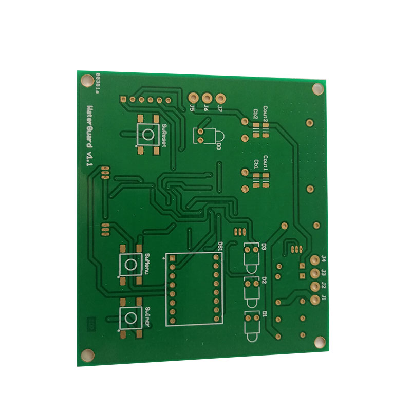
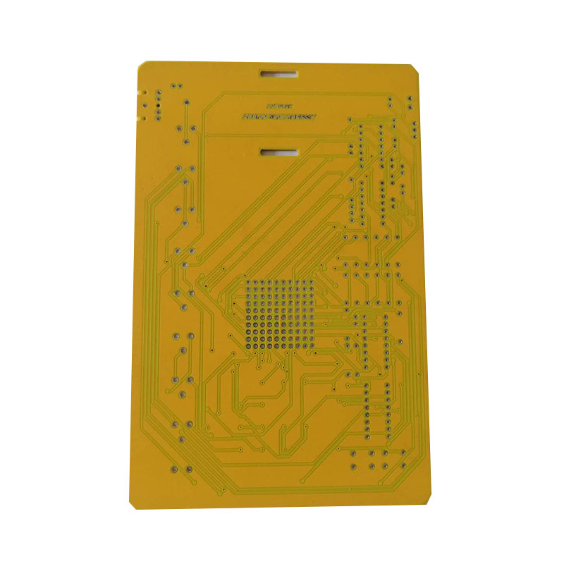
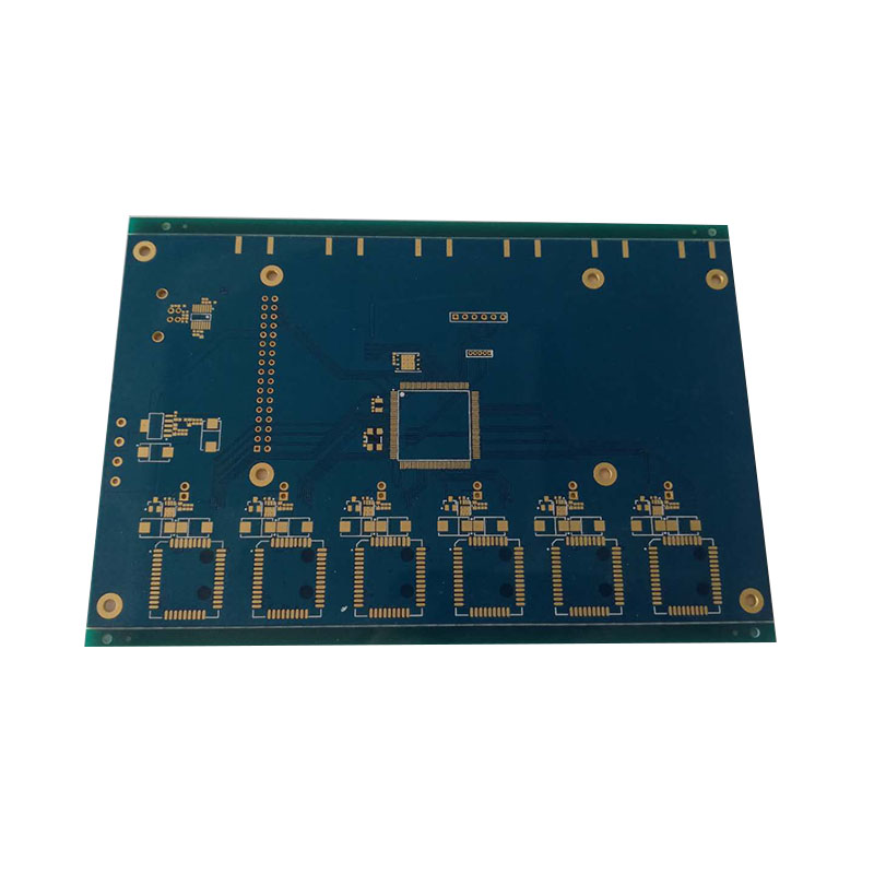
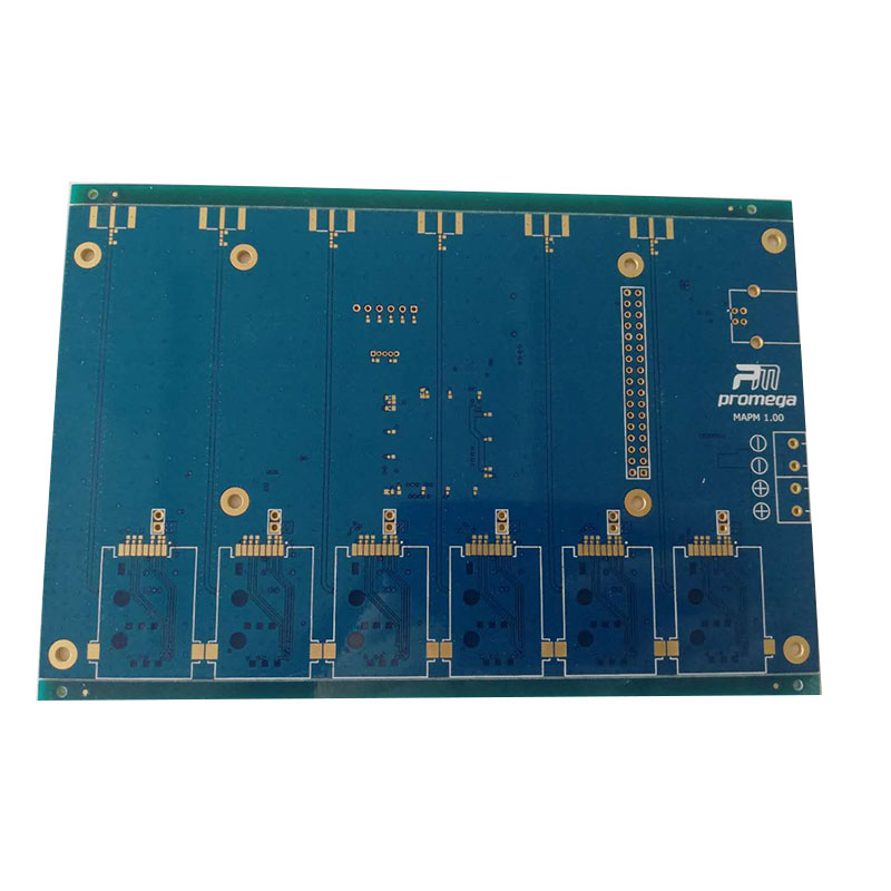
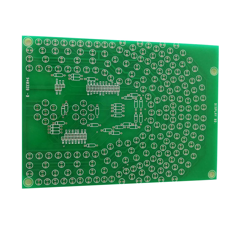
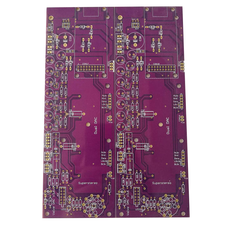
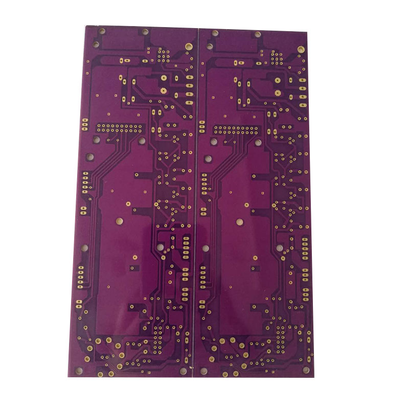
PCB multilayer is a multilayer circuit board used in electrical products. Multilayer boards use more single or double panel wiring boards.With a double lining, two one-way for outer layer or two double lining, two blocks of single outer layer of the printed circuit board, through the positioning system and alternate insulation adhesive materials and conductive graphics interconnection according to design requirement of printed circuit board becomes four, six layer printed circuit board, also known as multilayer printed circuit board.
With the continuous development of SMT (surface mounting technology) and the continuous introduction of new generation OF SMD (surface mounting devices), such as QFP, QFN, CSP, BGA (especially MBGA), electronic products have become more intelligent and miniaturized, thus promoting the major reform and progress of PCB industrial technology.Since IBM first successfully developed high density multilayer (SLC) in 1991, various groups in various countries have also developed various high density Interconnection (HDI) microorifice plates.With the rapid development of these processing technologies, PCB design has gradually developed to the direction of multi-layer and high-density wiring.With its flexible design, stable and reliable electrical performance and superior economic performance, multilayer PCB has been widely used in the production and manufacturing of electronic products.
The biggest difference between PCB multilayer and single panel and double panel is the addition of internal power layer (maintaining internal power layer) and ground layer. The power and ground network is mainly wired on the power layer.However, multi – laminate wiring is mainly based on the top and bottom layer, supplemented by the intermediate wiring layer.Therefore, the design method of multilayer board is basically the same as that of double panel, and the key lies in how to optimize the wiring of internal electrical layer, so that the wiring of circuit board is more reasonable and electromagnetic compatibility is better.
How are laminates laminated?
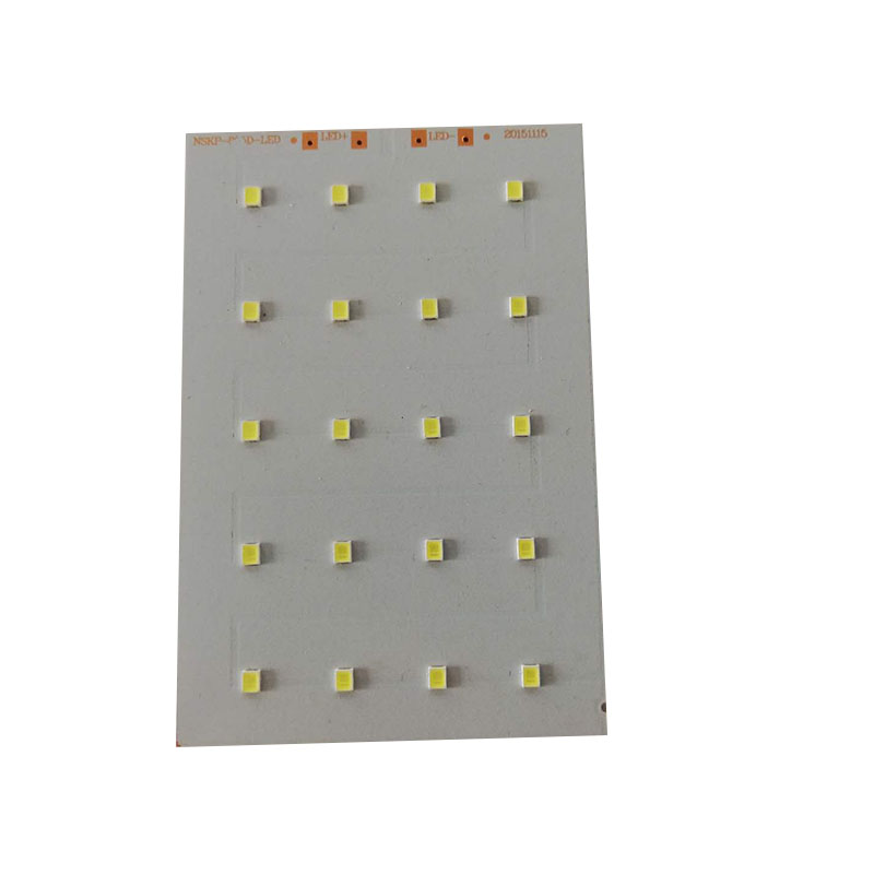
Aluminum pcb for a variety of electronic components, integrated circuits provide fixed, electronic components of the mechanical support components, is to achieve the electrical connection of the assembly plate. Aluminum based circuit board is called printed circuit board or printed aluminum based circuit board, PCB English name. The aluminum base circuit board itself is the insulation base board, the aluminum base board assembly mounting hole, the connection wire (copper), the board welding electronic component pin welding assembly. Electronic components are mounted on one side of the aluminum-based circuit board and pins are used for welding components on the other side. A layer of insulating paint is often applied to the welding surface. Both positive and negative al-based PCB manufacturers often have graphic symbols and the number of electronic components, but only the components mounted on the surface of the al-based PCB manufacturer are provided with graphic symbols and Numbers.
Meet the Dream Team
Textile inspires and equips people to accelerate sustainable practices in the textile value chain. We focus on minimizing the harmful impacts of the global textile industry and maximizing its positive effects.

Lamination, as the name suggests, is the process of bonding the various layers of line sheets into a whole. The whole process, including kissing pressure, full pressure, cold pressure. During the kissing stage, the resin wets the bonding surface and fills the gaps in the circuit, then enters full pressure to bond all the gaps. The so-called cold pressing is to make the circuit board cool quickly and keep the size stable.The matters needing attention in the lamination process, first of all, in the design, must meet the requirements of the lamination of the inner core board, mainly thickness, external dimensions, positioning hole The design should be carried out according to specific requirements. In general, the inner core plate requires no opening, short, open circuit, no oxidation and no residual film.
Secondly, when laminated, the inner core plate shall be treated with black oxidation treatment and Browning treatment. Oxidation treatment is to form a black oxide film on the inner copper foil, Browning treatment process is to form an organic film on the inner copper foil.
Finally, in the process of laminating, attention should be paid to temperature, pressure and time. Temperature, mainly to pay attention to the melting temperature and curing temperature of the resin, hot plate setting temperature, the actual temperature of the material and the change in temperature rate, these parameters need to pay attention to. As for the pressure, the basic principle is to fill the interlayer cavity with resin and exhaust the interlayer gases and volatiles. The time parameters mainly include the control of pressurization time, heating time, gel time, etc.


What are the basic principles of impedance and cascade design considerations for multilaminates?
Answer: In impedance and cascade design, the main basis is PCB board thickness, layer number, impedance value requirements, current size, signal integrity, power integrity, etc. The general principles of reference are as follows: L laminated layer has symmetry; L Impedance has continuity; L The reference layer below the component surface should be a complete ground or power source (generally the second or penultimate layer); L Power supply plane is tightly coupled to the ground plane; L signal layer as close as possible to the reference plane layer; L Separate the two adjacent signal layers as far as possible. The running line is orthogonal; The upper and lower reference layers of L signal are ground and power source, so as to shorten the distance between the signal layer and the formation as much as possible; L Difference signal spacing ≤2 times line width; The semi-cured sheets between l plates are ≤3;