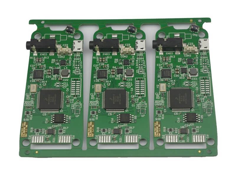
Panel refers to a small PCB board to let the manufacturer directly into a whole block.
A. Why do we need to put together the board, that is, what are the benefits of putting together the board?
1. To meet the needs of production. Some PCB boards are too small to meet the requirements of fixtures, so they need to be put together for production.
2. To improve the SMT placement of welding efficiency. Only need to pass SMT once to complete the welding of multiple PCBs.
3. improve cost utilization. Some PCB boards are shaped, the patchwork can be more efficient use of PCB board area, reduce waste and improve the utilization of costs.
Second, what are the several ways to design the board together?
V-CUT is to draw a slot in the connection of two boards, as long as the two boards together, leaving a gap between them (generally 0.4mm), but the connection of the board in this place is relatively thin, easy to break, when the board needs to be combined with the edges of the two boards.
V-CUT is generally straight, there will be no bending arc and other complex alignment, in the spelling board as far as possible in a straight line.
2. Stamp hole
For irregular PCB boards, such as round, V-CUT can not do, this time it is necessary to use to stamp holes to connect the board, so stamp holes are generally used more in the shaped board.
The edges of the two boards are connected by a small piece of plate, and this small piece of plate has many small holes at the connection of the two boards, so it is easy to break. After breaking, the edge of the board resembles the edge of a postage stamp, so this type of paneling is called a stamp hole.
3. Hollow joint strip
The hollow joint strip is used more often in the boards with half-hole process, which uses very narrow boards for jointing, somewhat similar to the stamp hole, the difference is that the joint part of the joint strip is a little narrower, and there is no over-hole on both sides.
There is one disadvantage of the hollow joint method: the board will have a very obvious bump after breaking. The stamp hole also has a bump, but it is not so obvious because it is separated by the overholes.
Some people may think that it is better to use the stamp hole directly, why do you need to use the hollow joint strip? This is because when the module is surrounded by half holes, the stamp hole and V-CUT can not be used, only through the hollow connection strip in the four corners of the module to connect.
Third, what is the principle of assembling boards?
In order to facilitate production, keep the square shape of the board after piecing as much as possible. In short, do not let the length and width ratio gap is too big.
Fourth, the spacing requirements.
1. for the outermost component from the edge of the board <3mm PCB must be added to the process edge, usually the longer side as the process edge.
2. Components and V-CUT should be reserved between > 0.5mm of space to ensure the normal operation of the tool.