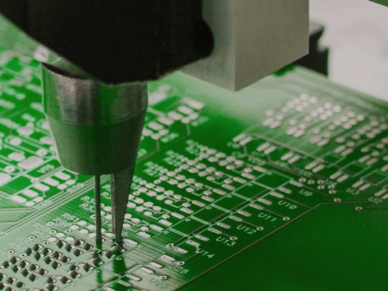
PCB circuit board is widely used in today’s various fields of electronic products, is one of the indispensable components of electronic products, is also the component carrier of each electronic products.Because PCB boards are copper-clad boards, tin or nickel-gold is the most commonly used process to solder the copper wires together with the pins of the components.The following circuit board bgpcba manufacturer mainly introduces the advantages and disadvantages of PCB circuit board precipitation process:
First of all, the reason why the gold precipitation process is covered on the PCB pad, as an important part of PCBA, must be because nickel gold is very easy to weld together with tin, and nickel gold can also play a role in protecting the copper sheet of the pad from air oxidation and corrosion, to protect the circuit board.
In addition, the nickel gold process is in line with the environmental protection requirements advocated by various countries. The gold sinking technology is a lead-free process, and customers can rest assured of the use of production.Zedoary zedoary process because it is chemistry, so covering on the surface of the welded plate, gold are both flat, it is also very easy to welding, especially now that a lot of high precision circuit boards, BGA processing requirement is very high, if caused the poor welding welding, BGA is not so good to find the reason, cause the PCB circuit board factory engineer adjustment is also a trouble,So gold process, generally can be very good to avoid this phenomenon, so now many precision circuit boards are using gold process to do only.
However, there is a drawback to the gold sinking process, that is, the cost will be more expensive than the general process.As the cost of the company, generally not very precise or high requirements of the board, you can choose to spray lead tin or lead-free tin.
Why used gold plates?
In order to solve the above problems of gold-plated plate, PCB with gold-immersed plate mainly has the following characteristics:
1, because the crystal structure formed by gold and gold plating is not the same, gold will be gold gold is more yellow than gold plating, customer satisfaction.
2, because the crystal structure formed by gold and gold plating is not the same, gold is easier to weld than gold plating, will not cause poor welding, cause customer complaints.
3.Because there is only nickel gold on the solder pad of the immersed gold plate, the signal transmission in the skin effect is in the copper layer, which will not affect the signal.
4, because the crystal structure of gold is denser than that of gold plating, and it is not easy to produce oxidation.
5, because there is only nickel gold on the welding pad of the immersed gold plate, so it will not be produced into gold wire caused by short.
6, because there is only nickel gold on the welding pad of the immersed gold plate, so the combination of welding resistance and copper layer on the line is more solid.
7, the project will not affect the spacing when making compensation.
8, because the crystal structure formed by gold and gold plating is not the same, the stress of the gold plate is easier to control, for bound products, more conducive to the processing of binding.At the same time, because the gold is softer than the gold plating, the gold plate is not wear-resistant.
9.The flatness and service life of the gold plate are as good as the gold plate.
