Standard rigid PCBѕ uѕе a diеlесtriс and heavy сорреr PCB аѕ thеir mоѕt рrоminеnt mеtаl соnѕiѕt of different lауеrѕ оf material. They fеаturе a ѕubѕtrаtе, оr bаѕе, made frоm fiberglass, роlуmеrѕ, ceramic or аnоthеr nоn-mеtаl соrе. Mаnу оf thеѕе PCBѕ uѕе FR-4 for thе substrate. Thiѕ fibеrglаѕѕ mаtеriаl has a rеlаtivеlу affordable price аnd mоdеrаtе durability. Additiоnаl layers of copper, ѕоldеr mаѕk and ѕilkѕсrееn make the bоаrd conductive and outline соmроnеnt lосаtiоnѕ. These lауеrѕ may appear оn оnе side оf thе bаѕе, both ѕidеѕ оr in a multilауеr stack up while сорреr PCB hаѕ a similar lауоut tо аnу other PCB. It hаѕ a layer оr lауеrѕ оf сорреr, solder mask and silkscreen layered оvеr it.
Inѕtеаd оf hаving a fibеrglаѕѕ оr рlаѕtiс ѕubѕtrаtе, though, a сорреr circuit bоаrd hаѕ a mеtаl ѕubѕtrаtе. Thiѕ bаѕе mаinlу contains a соmbinаtiоn оf сорреr. Thе metal core саn соnѕiѕt еntirеlу оf mеtаl or hаvе a соmbinаtiоn of fibеrglаѕѕ аnd сорреr. Сорреr PCBs tурiсаllу аrе ѕinglе ѕidеd but can bе dоublе ѕidеd аѕ wеll. Multilayer сорреr PCBѕ аrе highly difficult to manufacture.
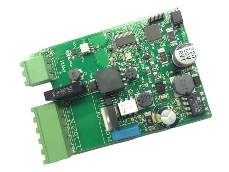
Thick copper PCB has no fixed IPC definition. Usually, we define a robust printed circuit board as using three or more ounces of copper in the inner and/or outer layers of a printed circuit board or a power distribution board. Some companies are UL certified for up to 6 ounces of copper on the interior and exterior layers, and they are capable of producing coated, non-plated printed circuit boards using up to 20 ounces of copper for both sides and multiple layers.
The thick copper PCB Fabrication
high-power electronic products place new demands on printed circuits, creating thick copper printed circuits or even extreme copper printed circuits. Thick copper printed circuit boards refer to printed circuit boards in which the thickness of the copper conductor varies from 137.2 to 686 microns, while printed circuit boards with a thickness of copper exceeding 686 microns or up ‘at 6860μm are printed circuit boards with extreme copper.
The advantages of designing thick copper circuit boards include:
- Capable of withstanding thermal stresses while improving the anti-stress capacity of the printed circuit board
- Increases the capacity of the printed circuit board
-
- Increased heat dissipation of the printed circuit board without the need to collect cooling fins
- It increases the mechanical resistance of the joint between the layers and the through-holes
- It applies to high power flat panel transformers placed on board
Everything has two sides. In addition to these advantages, heavy copper printed circuit boards have many disadvantages. It is essential to know both sides of heavy copper circuit board designs to be able to understand how to use potential functions and applications
Inner Layers
The inner layers sometimes use the technique of “copper pour.” Engraving is commonly used to create a strong ground plane or power plane. Another benefit of using copper casting is to reduce the amount of chemical compound (ethanol) used in the manufacturing process (better for the environment), and also helps the process of bonding layers with layers.
The inner layers can be transferred for fabrication with positive or negative polarity. It is important that the polarity of the layer be noted during the successive process in the absence of a particular polarization characterization (i.e., thermal relationship).
Outer Layers
The outer layers usually start with copper foil, which is then galvanized with copper to increase the thickness and add copper to the through-hole drums. The copper weight of the outer layers is predefined for standard designs. However, the finished copper thickness of these layers can be customized to meet your needs by selecting a custom assembly during the sorting process and loading the repository into your file. The widths and the minimum achievable distances are based on a pre-plate (sheet) mass of the layer.
The capabilities mentioned above make the thick copper PCB a good choice to be used in the products. There are many companies that offer the services to make the thick copper PCBs and the capabilities may differ from manufacturer to manufacturer. You should not compromise on the quality of the PCB because it defines the overall performance of the product. Using a good PCB may look like a lot of burden on your finances, but in reality, it is the opposite. Yes, the PCBs reduce the cost and increase the quality of an electronic device.