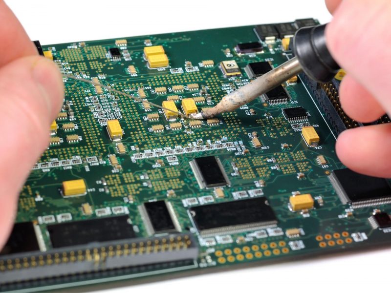
Common pads are “common diseases and frequently-occurring diseases” in PCB design, and are also one of the main factors causing hidden dangers in PCB soldering quality.
- After soldering the chip components on the same pad, if the pin-inserted components or wiring are soldered again, there is a hidden danger of soldering during the second soldering.
- Limits the number of repairs for subsequent commissioning, testing, and after-sales repairs.
- When repairing, one component is removed soldering, and the components around the pad are removed too.
- When the common pad is used, the stress on the pad is too large, causing the pad to peel off during soldering.
- The same pad is shared between the components, the amount of tin is too much, the surface tension is asymmetrical after melting, and the components are pulled to one side to generate displacement or tombstoning.
- Similar to the non-standard use of other pads, the main reason is that only considering the circuit characteristics and the area or space limitation, many component installations, solder joint defects, etc. occur in the assembly soldering process, and finally cause great impact on the reliability of the circuit operation.
