The copper layers are essential to carry electricity throughout your PCB. Depending on the purpose, PCBs have a simple or complex design. Apart from the foundation layer of the substrate, copper layers are another essential component.
Your PCB cam comes with a single layer of copper applied to the top or two layers on both sides of the substrate. The PCB can also have numerous layers with other copper and substrate. Some PCBs used in advanced devices or smartphones have more than 12 or 16 layers of copper.
Copper layers are much lesser in width than the substrate layers, and you won’t have any electricity flowing through your circuit if they are absent.
The manufacturer can use a combination of different methods to bond the copper to the surface of the substrate. Standard methods involve heat, pressure, and adhesive so that the copper layers are fixed firmly on the substrate. You can take your PCB for drilling after the copper has bonded with the substrate.
For your device to function, the PCB needs to transmit the charge to the right points from one layer to another layer in the board. You will have to create holes referred to as via for the cost to flow through. The manufacturer has several options to drill holes on the PCB and use a CO2 laser, UV laser, or other equipment.
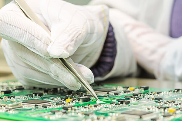
The accuracy and efficiency of the drilling machine determine the preciseness and complexity of the PCB.
You have to clean the holes of any debris or any material that might have been left behind after the process of drilling. They can also be deburred to get any additional material clinging to the PCB. After that, the inner sides of the vias are coated with copper to carry the charge from one layer of the circuit board to another.
Next, you have to print the pattern of the circuit on the PCB. The manufacturer can deploy the copper accurately following the design to get the way on board. Otherwise, they may apply copper to the entire board and then remove the copper to etch out the circuit pattern.