The application of ident layers during PCB color and manufacturing is referred to as silk screening. So what is PCB silkscreen? Silk screening is used as components for identifying their testing points, PCBA part numbers, company information, manufacturer notes, and so on. You can also define silk screening as the process of writing human-readable text-based information on the printed circuit board.
The process of silk screening requires the implementation of formulated conductive inks. Then standard colors typically used for the silk screening methods include yellow, white, and black. It is to be noted that you can request for non – traditional colors for the process, but they will cost you much time, money, and energy.
Another thing that is very important and requires to be considered during silk screening is font selection. There was a time when the only software used was for fonts was PCB CAD, but now there is a wide range of options available. Ensure that you are selecting a font that the readers easily understand. Some fonts may seem exciting but are hard to be recognized and give problems in reading.
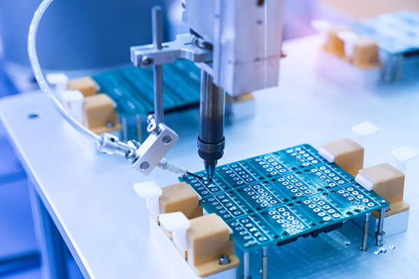
The silkscreening process today is still using traditional and conventional methods. The process of silk screening is performed by stretching polyester screens across the frames of aluminum. Before the step of imaging, the coating of screens is performed using solvent-resistant emulsions.
It is to be noted that there must be proper alignment between the screen and panel. While the equipment required by this silk screening process is a laser photoplotter, spray developer, and ultraviolet printer are known as UV printers. A laser photoplotter is therefore used for producing the initial film. Screens can be reclaimed and can be cleaned again. However, the reuse of screens is not recommended for high resolutions.