July 14, 2023
WHAT IS A PCB STACKUP?
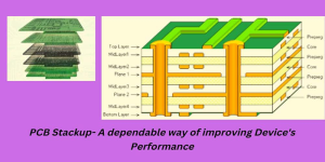
The most convenient way to arrange the PCB layer (Copper and insulating layer) is PCB stackup. This is the earlier step of PCB layout designing.
Usually, PCB stackup is related to PCB layers, PCB vias, prepregs, cores, lamination process, etc. It ensures impedance stability, minimization of EMI, and premium functional properties, along with the standard durability of electronic devices.
HOW DO I SELECT A PCB STACKUP?
Usually, multilayer PCB stackup is preferable for electric circuits. There are some criteria to choose the best stackup. Such as
- Flawless design
- Layer alignment
- Proper placement of PCB vias
- Improved thermal management system
- Compatibility with advanced electronic applications
- High-quality materials
- Standard lamination
- Reducing EMI and signal noise
- Easy and rapid repairing
- Affordable cost
- Advanced functionality and durability
- Manufactured by a high-class PCBA manufacturer
THE DIFFERENCE BETWEEN STANDARD PCB STACKUP AND HDI STACKUP
The main issues that differentiate standard PCB stackup and HDI (High-Density Interconnect) stackup are-
Design challenge
Designing an HDI stackup is more challenging than that of a standard stackup.
Power consumption
HDI stackup offers comparatively lower power consumption than a standard PCB stackup of high layer count. That’s why HDI PCBs have extensive use in smartphones, batteries, etc.
Component placement
HDI stackup allows the manufacturer to place the components on both sides. But all standard PCB stackups are not compatible with this type of component placement. This feature makes HDI circuit boards lightweight and small.
Durability
HDI circuit boards come with higher thermal management. That’s why the durability and functionality are improved in HDI stackups compared to traditional PCB stackups.
Cost
Standard stackup of circuit boards offers an affordable cost in most cases. Ut, HDI stacks of type IV, type V, and type VI are highly expensive.
RULES FOR PROPER PCB STACKUP DESIGN
To get a well-designed PCB stackup, you need to follow some rules strictly. Such as
- Use the ground planes properly. The use of these planes protects the circuit board stackup from ground noise, as ground planes offer a reduced ground impedance.
- Ground planes can route the signals to strip lines. So, incorporate ground planes in your design.
- Place the signal layers and planes close, as much as possible.
- Apply a symmetric configuration for the PCB stackup design.
- Route the high-speed signals to the layers which are placed in between different levels.
- Ensure that the signal impedance in all layers is properly set.
- Set the signal layer thickness perfectly.
- Collect the PCB materials from a reliable source.

TIPS FOR PCB STACKUP DESIGN
As we have already mentioned the basic rules for an effective PCB stackup for electronic applications, you are familiar with this process. Here, we are going to share some tips with you so that the stacking process of PCB becomes convenient for the manufacturer.
Let’s have a look-
Tips for finding the number of layers
- Calculate the pin density. You can use the following equation in this case-
- Use a lookup table to determine the total number of PCB layers, along with finding the signal layers.
- Don’t mix the signal layers with other layers.
- Consider the power and frequency ratings while determining the layer numbers for PCB stackup.
Tips for layer arrangement
- Keep the signal layers adjacent to the power layers. It provides a strong coupling between the layers.
- Never place two signal layers next to each other
- Keep a minimum distance between the power and ground layers.
- Microstrips with low thickness require high-speed routing
Tips for selecting layer materials
- Choose the materials having appropriate thickness
- Check electrical, thermal, and mechanical properties
- Check the thickness of prepreg and cores.
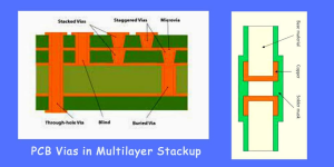
Tips for via placement
- Don’t incorporate blind or buried vias in the case of using through-hole vias for fan-out
- Set the PCB viaconcerning their rated currents.
| PCB Via | Current Rating |
| Through-hole Via | 1A |
| Blind Via | 300mA |
| Buried Via | 950mA |
- Never place through-hole vias with PCB components located under the BGA fan-out.
- Keep the air gap within 9mm while dealing with buried and blind vias.
-
PCB STACKUP DESIGN TOOL
A worthwhile design tool will increase the probability of getting a faultless PCB stackup. So much design software is used in the manufacturing world. For example,
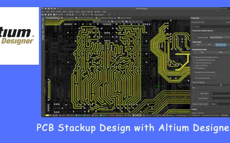
Altium Designer, KiCAD, Eagle, etc.But Altium Designer is the perfect and complete software for professional PCB stackup.
HOW TO DESIGN PCB STACKUP WITH ALTIUM DESIGNER?
- As a rules-driven design software, Altium is compatible with signal integrity tools and CAD tools. That’s why impedance control becomes easier.
●It enables the routing tools to receive data from the stackup directly. This property improves the circuit board quality to a certain extent.
●Altium is integrated with a field solver that helps calculate propagation delay.
●Altium offers a layer stack manager that is highly effective to choose high-quality PCB materials.
HOW TO PLAN MULTILAYER PCB STACKUP?
When you are dealing with a multilayer PCB stackup, you must plan for some issues. Like-
Material selection
You need to use dielectric materials like FR4, Epoxy resin, etc. You can find FR4 as both core and Prepreg.Impedance control
It’s a crucial issue in PCB stackup. You must have a plan for using a solder mask and conformal coatings as they affect impedance to a large extent.Layer management
- Keep the signal layer number between planes within two.
- Don’t place other layers between the plane and signal layers.
- Use a signal layer between the top and bottom.
- Don’t forget to establish a return path for signals.
Cost minimization
You can minimize the cost of multilayer PCB stackup through-- Using the PCB vias wisely
- Sourcing the proper dielectric materials
- Using the right number of layers for your application
- Considering the signal frequency and component density while designing the stackup
PCB STACKUP EXAMPLE

The most common and useful examples of PCB stackups include-
- 2 layer PCB stackup
- 4 layer stackup
- 6 layer stackup
- 8 layer stackup
- 10 layer PCB stackup
- 12 layer stackup
- 14 layer stackup
- 16 layer stackup
- 20 layer PCB stackup
- 32 layer stackup
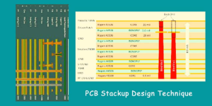
Do you know how to arrange the layers in the case of PCB stackup?
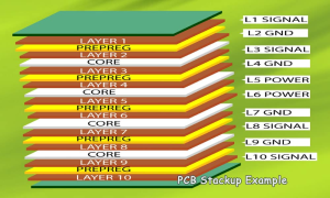
Let’s see the arrangements for 8 layers stackup.
- Top layer
- Prepreg
- Ground plane
- Core
- Inner layer
- Prepreg
- Power plane
- Core
- Ground plane
- Prepreg
- Inner layer
- Core
- Power plane
- Prepreg
- Bottom Layer
- As a rules-driven design software, Altium is compatible with signal integrity tools and CAD tools. That’s why impedance control becomes easier.