Designing a connector pinout for your PCB is an essential task that requires careful consideration of your project’s specific requirements and constraints. A well-thought-out pinout ensures the efficient and reliable performance of your electronic device, while also facilitating manufacturing and maintenance. In this detailed guide, we will walk you through the process of designing a connector pinout for your PCB, covering all the necessary steps, considerations, and best practices.
Understanding the Basics of Connector Pinouts
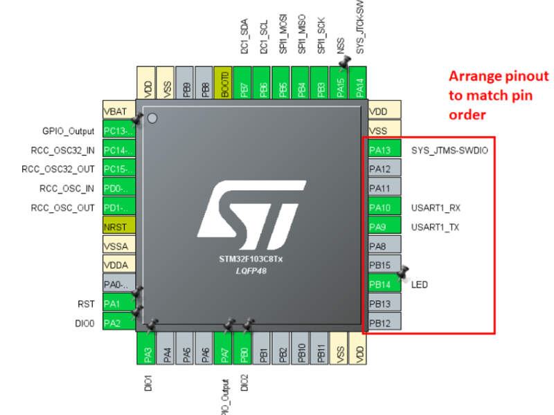
A connector pinout refers to the arrangement and configuration of the pins in an electrical connector. It defines how the pins are connected to the PCB and what functions they serve, such as power, ground, or data transmission. The pinout is crucial for ensuring that the connector mates correctly with its corresponding component and that the signals are transmitted accurately and efficiently.
Step 1: Define the Requirements
Before you begin designing the pinout, it’s essential to have a clear understanding of what your connector needs to achieve. Consider the following:
- Functionality: What is the purpose of the connector? Will it be used for power, data, or a combination of both?
- Number of Contacts: How many pins will be needed to support the required functions?
- Physical Space: What are the size constraints of the PCB and the connector?
- Environmental Factors: Will the connector be exposed to extreme temperatures, humidity, or other environmental stressors?
- Industry Standards: Are there any standard pin configurations that you should adhere to?
Step 2: Choose the Right Connector Type
There are various types of connectors available, each with its own advantages and limitations. Some common types include:
- Header and Socket: These are suitable for PCB-to-PCB connections or for connecting components like sensors and displays.
- Plug and Jack: Often used for external connections, such as audio and power cords.
- Pin Headers: These are used for making connections within the PCB or to other components.
Consider the following when selecting a connector type:
- Mating Mechanism: How will the connector be attached or detached? Push-fit, screw-lock, or latch mechanisms are common options.
- Signal Integrity: If high-speed data transmission is required, choose a connector with features like shielding or impedance control.
- Durability: Consider the number of mating cycles the connector will need to withstand.
Step 3: Design the Pin Configuration
Once you’ve chosen the connector type, it’s time to design the pin configuration. This involves determining the layout of the pins and assigning each pin a specific function. Consider the following:
- Pin Spacing: The distance between pins can affect the ease of assembly and the reliability of the connection. Standard spacings include 0.1″ (2.54mm), 0.05″ (1.27mm), and 0.025″ (0.635mm).
- Pin Orientation: The orientation of the pins (straight, right-angle, or vertical) can impact the ease of connection and the overall design of the device.
- Grounding: Ensure that there are sufficient grounding connections to minimize electrical noise and provide a stable reference point.
Step 4: Material Selection
The choice of materials for the connector and the PCB traces can significantly impact the performance and reliability of the pinout. Common materials include:
- Copper: The standard material for PCB traces, known for its excellent conductivity.
- Gold Plating: Often used for high-reliability applications due to its resistance to corrosion and excellent conductivity.
- Phosphor Bronze: A popular choice for connectors due to its durability and good spring properties.
Step 5: Consider Thermal Management
Electronic components can generate heat, which can affect the performance and lifespan of your device. When designing the pinout, consider the following thermal management strategies:
- Heat Dissipation: Use materials and design features that facilitate heat transfer away from critical components.
- Airflow: Design the layout to promote proper airflow around the connector and other heat-generating components.
Step 6: Design for Manufacturability
A pinout that is easy to manufacture will save time and reduce costs. Consider the following when designing for manufacturability:
- Tolerances: Allow for reasonable manufacturing tolerances to ensure a good fit between the connector and the PCB.
- Solderability: Design the PCB pads and traces to be compatible with the intended soldering process.
- Testability: Ensure that the pinout allows for easy testing of the connections and troubleshooting of potential issues.
Step 7: Document and Validate the Pinout
Once the pinout is designed, it’s crucial to document it thoroughly and validate its functionality:
- Pinout Diagram: Create a detailed diagram that clearly shows the pin assignments and their functions.
- Bill of Materials (BOM): Compile a list of all the components required for the connector assembly.
- Prototype Testing: Build a prototype and perform tests to ensure that the pinout functions as intended under various conditions.
Step 8: Review and Iterate
After the initial design and testing, it’s essential to review the pinout with a critical eye:
- Peer Review: Have other engineers or designers review your pinout for potential improvements.
- Feedback Incorporation: Make any necessary changes based on the feedback received and retest the pinout as needed.
Conclusion
Designing a connector pinout for your PCB is a complex process that requires a deep understanding of your project’s requirements and constraints. By following the steps outlined in this guide and considering the various design aspects, you can create a pinout that is not only functional and reliable but also easy to manufacture and maintain. Remember that attention to detail and a methodical approach are key to achieving a successful design. With careful planning and iteration, your connector pinout will serve as a solid foundation for your electronic device, ensuring its performance and longevity.
Creating a connector pinout table is a great way to visualize and document the function and configuration of each pin in a connector. This table can serve as a reference for engineers, technicians, and even for those troubleshooting or modifying the design. Below is an example of a connector pinout table, which can be used for a variety of connectors, such as USB, HDMI, or a custom I/O connector for a specific application.
.. | … |
| Pin Number | Function | Description | Voltage | I/O |
|————|—————-|———————————————|———|—–|
| 1 | VCC | Positive supply voltage | 5V | Out |
| 2 | GND | Ground reference | GND | In |
| 3 | TXD | Transmit data signal | N/A | Out |
| 4 | RXD | Receive data signal | N/A | In |
| 5 | CTS | Clear to send signal (flow control) | N/A | In |
| 6 | RTS | Ready to send signal (flow control) | N/A | Out |
| 7 | DTR | Data terminal ready | N/A | Out |
| 8 | DSR | Data set ready | N/A | In |
| 9 | RI | Ring indicator | N/A | In |
| 10 | CD | Carrier detect | N/A | In |
| 11 | PWR LED | Power indicator LED (optional) | 5V | Out |
| 12 | LINK LED | Link status LED (optional) | 5V | Out |
| 13 | TX LED | Transmit activity LED (optional) | 5V | Out |
| 14 | RX LED | Receive activity LED (optional) | 5V | Out |
| 15 | NC | No connection (not connected) | N/A | NC |
| 16 | NC | No connection (not connected) N/A | NC |
Legend:
- Pin Number: The numerical position of the pin in the connector.
- Function: The name or label of the pin, indicating its role in the circuit.
- Description: A brief explanation of what the pin is used for or its purpose.
- Voltage: The voltage level associated with the pin, if applicable. ‘N/A’ indicates that the pin is not associated with a voltage signal. ‘GND’ represents the ground potential.
- I/O: The direction of the signal (Input ‘In’, Output ‘Out’, or No Connection ‘NC’).
This table provides a clear and concise overview of the connector’s pinout. It is important to note that the actual pin count and functions will vary depending on the specific connector being designed. This table is just an example and should be adjusted to fit the requirements of the particular connector in question. Additionally, for more complex connectors or systems with multiple protocols or functionalities, the table may need to include more rows and columns to accurately represent all necessary information.