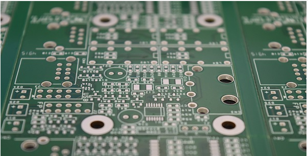
A PCB footprint is a standardized component outline on a printed circuit board (PCB). The design contains all the information needed to place the component on a board.
A PCB footprint describes two-dimensional features of an object in three-dimensional space. It is similar to a mechanical CAD drawing but includes only the information available for printing on the copper layer.
A PCB footprint contains:
- The location of pads and pins (if applicable).
●Dimensions and tolerances for these pads and pins.
●A description of other features, such as mounting holes or standoffs, ensures proper spacing between components.
WHAT ARE THE TYPES AND DIMENSIONS OF PCB FOOTPRINTS?
There are several types of PCB footprints. The most common ones are:
- SOP (Small Outline Package)— This is the smallest footprint used for integrated circuits (ICs). It’s usually about 0.4″ x 0.4″.
●QFP (Quad Flat Package)— This larger PCB footprint is used for ICs and integrated circuits. It’s usually about 0.8″ x 0.8″, but can be as large as 1″ x 1″.
●BGA (Ball Grid Array) — This is an even larger PCB footprint for ICs and integrated circuits with many connections. They’re usually rectangular with pins on all sides, so they can be placed in any direction without worrying about orientation. Their size varies widely depending on how many connections per IC; sizes range from 0.5″ x 0.5″ to over 2″ x 2″.
THE STANDARDS FOR PCB FOOTPRINT
IPC-7351 (Recommended Practice for the Design, Manufacture, and Assembly of Printed Boards) is a standard published by the Electronics Industry Association that defines requirements for PCB design and manufacture. It specifies the technical details of designing and producing a PCB footprint.
WHAT ARE THE RULES FOR PCB FOOTPRINTS?
Here are the main rules for creating a PCB footprint:
- Place parts in the center of the copper layer. This will reduce the amount of etching needed on the board, which increases its efficiency and reduces cost.
●Don’t leave large areas empty between parts. This wastes space on boards and makes them less efficient than they could be.
●Keep track of all components used in your design so you can reuse them easily when making changes later.
WHY ARE PCB FOOTPRINT RULES REQUIRED?
PCB footprint rules are required to ensure that the PCB is designed properly and that it is not going to cause any harm to the user. The PCB footprints are a reference point for placing components on the board. This helps in avoiding mistakes when placing components.
The standard rules and regulations help ensure that all PCBs have proper electrical connections between them so they can be used safely.
PCB FOOTPRINT CREATION GUIDELINES
The following are PCB footprint creation guidelines:
- Only the top layer should have footprints.
●It is best to create footprints in the center of the pad, not at the edge.
●The footprint size must be larger than the package outline by at least 3 mils (0.003 inches). This is so that any copper around the outer edge of the package will not short out against vias when mounting it to a board.
●Footprints should use pads that have no overlap with other pads (no “islands”). A via or inner plane separates power and ground pads. Reflow soldering requires isolation of each pad from others to prevent shorts between them.
●PCB footprints should use pads connected internally by a continuous trace or plane running through them all (no individual islands). This allows for them to be more easily soldered than footprints, where each pad has its separate trace leading back up to a top-side connection point on your board’s silkscreen layer (such as an IC pin).
HOW DO I GET A PCB FOOTPRINT?
There are several sources for PCB footprints. The best way to get hands-on with them is by purchasing them directly from an online vendor. Alternatively, PCB designers can find some free footprints online at places like SparkFun or OSHPark’s GitHub page.
When designers are looking for PCB footprints for a specific part, ensure that the vendor has provided all information required for each pin and pad so that your software can correctly populate it.
PROBLEMS WHEN PCB FOOTPRINT CREATION GUIDELINES ARE NOT IN PLACE
Many problems can arise when PCB footprint creation guidelines are not in place. These include:
Unnecessary rework
A designer who works on a board may be forced to do unnecessary rework because of poor design specifications or design rules. This is especially true for new designers or those who do not have much experience with the process. Good design guidelines allow them to follow the rules and easily create high-quality products.
Missed deadlines
When deadlines are missed, it can be very costly to a company. Not only does it make them lose money by missing out on sales opportunities, but it also affects their reputation. If customers are unhappy with their products, they may start looking elsewhere for similar ones that perform better and cost less money.
Incorrect parts used
Designers might choose incorrect parts for their designs when no documentation is available on creating PCBs. This can cause problems down the road because some parts may not work together properly and could cause failures during use or after installation.
HOW DO I CHECK MY PCB FOOTPRINT?
For checking PCB footprint, PCB Footprint Checker software is required.
The PCB layout software allows designers and manufacturers to find out how much space the components take on the board (for example, what percentage of the board is occupied by a specific component), which is helpful when planning the board size or choosing the right components.
Following are some popular tools to check PCB Footprint:
1. KiCad (Free)
2. Altium Designer (Paid)
3. EagleCAD (Free)