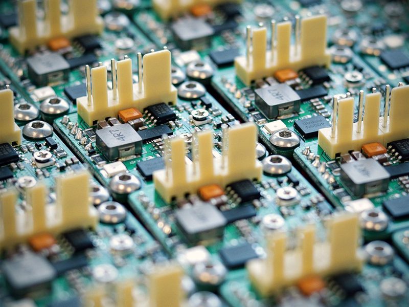
A printed circuit board (PCB) is a bridge connecting electronic components and circuits, serving as the backbone of electronic products. It is widely used in various fields such as communication, consumer electronics, computer, automotive electronics, industrial control, medical equipment, defense, and aerospace. It is an essential electronic component in modern electronic information products.
Since the mid-1930s, PCB has been invented for more than 80 years. History has proved that without circuit boards, there would be no electronic circuits, no flight, no transportation, no atomic energy, no computers, no space travel, no communication, and no home appliances.
The reason is easy to understand: chips and integrated circuits are the core of the electronic information industry, and semiconductor technology reflects a country’s level of industrial modernization, guiding the development of the electronic information industry. The electrical interconnection and assembly of semiconductors (integrated circuits, IC) must rely on PCB. So how are circuit boards made and what is the process like? Below we will explain it step by step for everyone.
PCB Design Basics
Printed circuit boards (PCBs) are used to connect electronic components in a wide range of devices, from consumer electronics to industrial equipment. Designing a PCB requires careful consideration of various factors to ensure that the final product is functional, reliable, and efficient. In this article, we’ll cover some of the basics of PCB design.
PCB Design Tools
To design a PCB, you will need a PCB design tool. There are many options available, both free and paid, with varying levels of complexity and functionality. Some popular options include Altium, Eagle, KiCad, and OrCAD.
PCB Layout
The PCB layout is the physical representation of the electronic circuit. The layout includes the placement of components, the routing of electrical connections between components, and the location of mounting holes and other features.
Component Placement
The placement of components is a critical aspect of PCB design. Components should be arranged in a way that allows for efficient routing of traces and minimizes the length of high-speed signal paths. Components should also be placed in a way that allows for proper heat dissipation and adequate clearance between components.
Trace Routing
Trace routing involves connecting the components on the board with conductive traces. The routing of traces should be done in a way that minimizes electromagnetic interference and noise. High-speed signals should be routed first, and they should be kept as short and direct as possible. Traces should also be wide enough to carry the necessary current without causing excessive resistance.
Ground Plane
A ground plane is a large area of copper that is connected to the ground signal. The ground plane is used to provide a low-impedance path for electrical currents and to reduce electromagnetic interference. A solid ground plane is generally preferred over a ground grid or a mixture of power and ground planes.
Power Plane
A power plane is a large area of copper that is connected to the power supply signal. The power plane is used to provide a low-impedance path for electrical currents and to reduce electromagnetic interference. It’s recommended to use separate power planes for different voltage levels to avoid any interference.
Design Rules
Design rules are parameters that define the minimum spacing, trace width, and other parameters to ensure that the PCB is manufacturable and reliable. The design rules may vary depending on the capabilities of the manufacturer and the technology used in the PCB fabrication.
Conclusion
Designing a PCB requires careful consideration of various factors, from the placement of components to the routing of traces and the definition of design rules. A well-designed PCB is critical for ensuring the functionality, reliability, and efficiency of electronic circuits. By following these PCB design basics, you can create a PCB that meets the required specifications and standards.
Before the PCB assembly process
there are several steps that should be taken to ensure a successful assembly process. Here are a few key steps:
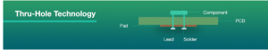
- PCB Inspection: The first step is to visually inspect the bare PCB for any defects, such as cracks, breaks, or scratches. This is important to ensure that the board is in good condition and ready for assembly.
- Solder Paste Stenciling: Solder paste stenciling is the process of applying solder paste onto the PCB before component placement. This is typically done using a stencil to ensure that the paste is applied evenly and accurately. The stencil should be aligned with the PCB and checked for any defects before applying the solder paste.
- Component Placement: Once the solder paste has been applied, the components are placed onto the PCB. This is typically done using a pick and place machine, which accurately places each component onto the PCB.
- Reflow Soldering: Reflow soldering is the process of heating the PCB to melt the solder paste and create a permanent connection between the components and the board. The temperature and time of the reflow soldering process should be carefully controlled to ensure that the components are properly soldered and not damaged.
- Inspection and Testing: Once the PCB assembly process is complete, the board should be inspected and tested to ensure that all components are properly soldered and that the board functions correctly. This includes checking for any defects or issues, such as shorts, opens, or misaligned components.
By taking these steps before the PCB assembly process, you can ensure that the board is in good condition, the solder paste is applied correctly, the components are placed accurately, and the board functions properly after assembly.
Actual PCBA manufacturer process steps.
The actual PCB assembly process can vary depending on the specific manufacturer and the type of components being used. However, here are some general steps that are typically involved in the PCBA manufacturing process:
- Solder Paste Application: The first step in the PCBA manufacturing process is the application of solder paste to the PCB. This is typically done using a stencil to ensure that the paste is applied evenly and accurately.
- Pick and Place: Once the solder paste has been applied, the components are placed onto the PCB. This is typically done using a pick and place machine, which accurately places each component onto the PCB.
- Reflow Soldering: Reflow soldering is the process of heating the PCB to melt the solder paste and create a permanent connection between the components and the board. The temperature and time of the reflow soldering process should be carefully controlled to ensure that the components are properly soldered and not damaged.
- Inspection: Once the reflow soldering process is complete, the board should be visually inspected for any defects or issues, such as misaligned components or solder bridges.
- Automated Optical Inspection (AOI): Automated optical inspection (AOI) is typically used to detect any defects or issues that may not be visible to the human eye. This includes things like missing or misaligned components, solder defects, and other issues that can affect the performance of the PCB.
- In-Circuit Testing (ICT): In-circuit testing (ICT) is a type of functional testing that checks the electrical performance of the PCB. This includes testing for things like shorts, opens, and other issues that can affect the performance of the board.
- Final Inspection: Once the PCBA manufacturing process is complete, the final product should be inspected to ensure that it meets all of the required specifications and standards.
After the Printed Circuit Board Assembly (PCBA) process

After the Printed Circuit Board Assembly (PCBA) process, there are several steps that can be taken depending on your specific needs. Here are a few possible options:
- Inspection: Before moving on to further steps, it’s important to conduct a thorough inspection of the assembled boards. This can be done manually or using automated inspection equipment to check for any defects, such as missing components or soldering issues.
- Testing: After inspection, testing can be performed to ensure that the assembled boards are functioning properly. This can involve functional testing or in-circuit testing, depending on the complexity of the board.
- Programming: If your boards require programming, this can be done at this stage. This can involve loading firmware or other software onto the boards using specialized equipment.
- Packaging: Once the boards have been inspected, tested, and programmed (if necessary), they can be packaged for shipment. This can involve using specialized packaging to protect the boards during transit.
- Quality Control: Finally, it’s important to conduct a quality control check on the finished boards to ensure that they meet your specific requirements and standards.
Overall, the specific steps taken after the PCBA process will depend on your specific needs and requirements. It’s important to work with a trusted PCB assembly service provider who can help guide you through the entire process and ensure that your boards are assembled and processed to the highest standards.
These are the general steps involved in the PCBA manufacturing process. However, the specific details of the process can vary depending on the specific manufacturer and the requirements of the project.