WHY TOOLING IS IMPORTANT FOR PCB MANUFACTURING
Most all printed circuit boards start with an electronic database. I say “most” because some of the time we do scan old films to recreate an old PCB design. The data format must be interpreted by software and manipulated by an engineer that can interpret the files but also “see” what they are looking at.
The experienced engineer must perform a Design for Manufacturing (DFM) review to determine if the PCB is manufacturable but also be able to recognize an error or short-coming in the data set for correction. For nearly every processing step of the PCB, there is a CAM engineering step needed for the success of the project through production. Engineering works closely with production to process the electronic files for ease of manufacturing.
Free Download: Top 5 Circuit Board DFM Issues
CAD engineering in itself is a specialty process. The engineering team is tasked with developing the tools needed for every process including imaging, plating, drilling, routing, and testing all the required tools needed at each step of the PCB manufacturing process.
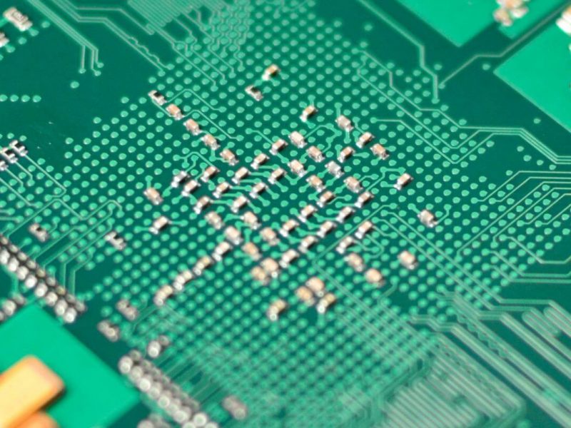
Repeated images within an array can save processing time at manufacturing and assembly.
Engineering
Engineering must determine the part/array square inch and location of each part within the master panel including coupons, thieving, text, targets, tooling holes, and optical alignment fiducials. All these items require strategic planning and placement within the usable area. The accuracy from the engineer’s programming skills to determine what is best for production is key for the success of production.
Manipulating the data without risk to the integrity of the PCB and adding processing factors needed to create the end result of quality circuit boards does not come without some risk and the process can be long, depending on the condition of the files received. During data processing, the CAM engineering team will interact directly with our customers to resolve any potential production issues upfront at the initial purchase order placement. The engineer will review all data to determine if there is any missing information needed for production and request by email additional documentation. At the same time, the engineer will also review for any missed steps at the quote level for review with the sales and planning teams.
Production engineering during the initial review for all of the different processes has a pre-determined set of guidelines for engineering to follow for the equipment, chemistries, labs, overage, and time to go. Without the key people in place, the product would not run smoothly, accurately, and on time from start to finish.
Master tooling includes coupons, tooling holes, targets, thieving, and other production aids.
PCB Production
The engineer must understand the PCB production process to accurately manipulate the database and work with the master panel sizes as defined by manufacturing.
The total size of the PCB laminate includes the individual PCBs and the tooling and waste area. The PCBs we consider the part size or array sizes vs the panel size. The part/array is the format in which the PCB is shipped to our customer. Single pieces or arrays are calculated into the usable space of the master panel. In most cases the usable area is the X,Y of the laminate minus a 1-inch or greater of the perimeter of the master, this one inch can vary for different suppliers or technology requirements.
The calculation of area is, for example, the most common master size of 24 inches by 18 inches, leaving the usable land at 22-inch by 16-inch area. The size of the deliverables is then calculated into the land area left over which equals the panel usage. The ideal piece or array size is 11 x 8 which would fit 4 up on the master panel or 6.5 x 4 would fit 8 times. Those sizes and quantities are optimum for usage. Keeping a higher percentage of used space allows for better cost. When a piece or array is even slightly larger say 11.5 x 8 the used area changed by 50%.
Processing
Understanding the area calculations and usage helps to understand the cost of tooling and panel usage loss. For all areas of production different items are needed to produce the parts. We will review several items needed and why.
Tooling holes for the first example of non-plated or plated holes used for production of the PCBs. They are added to the master panel for different processes to aid manufacturing with the process. For internal layers, holes are punched, pinned, drilled, or routed into the waste area edges for early-stage processing. For registration purposes, these holes are key for front-to-back inner-core imagery. Early stage panels are stacked and pinned for drilling purposes to allow for more than one panel to be drilled at a time. Registration holes, targets, coupons, and first/last drilled holes are placed within the 1-inch production area. These holes are used throughout the process to aid in the manufacturing of the parts, image, layup, mask, legend, drilling, and electrical test all require assistance holes.
PCB and Tooling Process
A PCB, or printed circuit board, is a mechanism that interconnects electronic components through conductive tracks and pads. The ways and places are etched from copper sheets laminated onto a non-conductive substrate.
Manufacturing these boards is not as simple as it may seem. The process involves creating several board prototypes, which can be expensive and time-consuming. This is where tooling comes in handy.
The tooling process is an initial setup stage for mass-producing circuit boards. In this stage, PCB manufacturers create PCB tools that will be used to produce copies of the original prototype during mass production.
This includes milling out the space for component insertion, drilling holes into the board and connecting them to appropriate layers using vias, and laminating any number of layers together to create multi-layer PCBs.
For every PCB project, tooling is essential to ensure production efficiency. It can be divided into three parts: preparation of stencil and support tooling, preparation of cutter and support tooling, and preparation of other special tools.
Preparation of Stencil and Support Tooling
The role of the stencil is to keep and transfer the solder paste onto the PCB board when using SMT components. Therefore, before preparing the stencil, we need to use software to create a solder paste file based on the PCB design files. After that, a stencil will be produced according to the file with a laser cutting machine.
Preparation of Cutter and Support Tooling
9 Reasons Why Is Tooling Important For PCB Manufacturing?
Cost Reduction
The main advantage of tooling is that it allows you to reduce the cost of manufacturing PCB assemblies significantly. Many companies use tools like stencils, cutting boards, or test fixtures to minimize their costs and maximize their profits.
The higher the number of manufactured PCB assemblies, the more considerable value has tools in the whole process! If you have a large order of 1000 pcs or more, you should consider making your tools!
Faster Assembling Time
If you are going to mass-produce PCB assemblies, it’s worth considering making customized tools like stencils or cutting boards that will precisely fit your board.
Reduce Material Waste
Circuit boards are typically expensive, and to minimize cost, the PCB manufacturer has to use as much of the board material as possible. The right set of tools will allow you to improve your layout so that all of the PCB material is used, which reduces costs and waste.
Optimize Performance
The proper tooling can optimize your design for low-power consumption, high-speed data transmission, and other critical performance metrics. It also helps you cross over different geometries while staying within budget and optimizing performance.