SMT (Surface Mount Technology) testing is a crucial part of PCB (Printed Circuit Board) production process. It ensures that all components of the board are properly placed and functioning as intended.
During SMT testing, automated machines scan the board for any faults or errors in the placement of components or soldering. Any defects found during this process are flagged and can be corrected before final assembly.
Without SMT testing, there is a risk that a faulty component may be installed on the board, leading to issues with functionality or even complete failure of the board.
Therefore, SMT testing is essential to guarantee the proper functioning of a PCB, and to avoid potentially costly rework or recalls.
How to test PCBA after SMT ?
- Visual inspection: A visual inspection of the board can be done to check for any obvious defects like misplaced components, soldering issues or any visual damage to the board. This method is usually performed manually.
- Automated Optical Inspection (AOI): AOI machines use cameras to inspect the board for defects such as component placement, polarity, and soldering quality.
- X-ray inspection: X-ray inspection can be used to examine hidden components, solder joints, and ensure proper connections between pins.
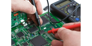
- In-Circuit Testing (ICT): ICT involves checking the electrical characteristics of the board by sending signals through the board’s traces and measuring their responses. It can detect issues such as short circuits or open circuits.
- Functional testing: This method involves testing the board’s functionality by simulating inputs and verifying the correct outputs. This method can help to ensure that the board is working as expected.
The choice of test method depends on various factors such as the complexity of the board, budget, volume of production, and customer requirements. A combination of different test methods can be used to ensure the highest quality of the PCBA.
PCB design and ICT test
Request PCBA Test Quote
PCB designs will be more complicated and difficult as electronic products get lighter and thinner. In addition to the need to balance functionality and safety, it also needs to be producible and testable. When designing the PCB, it is necessary to consider setting up ICT test points. The following are the precautions for ICT testing in PCB design:
- Although there is a double-sided ICT fixture, it is best to place the measured points on the same side.
- Priority stepsof tested points: A. Test-pad, Component Lead, C. Through-hole (Via).
- The center distance between the two measured points or the measured point and the pre-drilled hole should not be less than 0.050″ (1.27mm). It is better to be largerthan 0.100″ (2.54mm), followed by 0.075″ (1.905mm).
- The measured point should be at least 0.100″ away from the nearby parts (on the same side). For parts higher than 3m/m, the distance should be at least 0.120″.
- The measured points should be evenly distributed on the PCB surface to avoid local high density.
- The diameter of the measured point should be no less than 0.035″ (0.9mm). If it is on the upper needle board, it should be no less than 0.040″ (1.00mm). The shape is preferably square,and the measurable area is increased by 21% compared to the circle. The measured points less than 0.030″ need additional processing to correct the target.
- The pad and via of the tested pointsshould not have solder mask.
- The measured point should be at least 0.100″ away from the edge of the board or folded edge.
- The thickness of the PCB must be at least 0.062″ (1.35mm). PCBs with a thickness less than this value can be bent easilyand require special treatment.
- The diameter of the tooling hole is preferably 0.125″ (3.175mm). The tolerance should be “+0.002″/-0.001″and the position should be at the corner of the PCB.
- The position tolerance between the measured point and the positioning hole should be +/-0.002″.
- Avoid placing the measured point on the SMT part. Not only is the measurable area too smalland unreliable, but the part will damage easily.The measured point should not be greater than 0.170″ (4.3mm),and the aperture should be less than 1.5mm, or else it requires special treatment.
-
- ACI DIPparts feet are prioritized as test points.
- The exposed part of the copper foil (test PAD).
- Vertical parts DIP feet.
- Through-hole, but must not have mask.Information required for ICT fixture production:
- Layout CAD File: For example: PCADR–>* .pdf PADSR–> *.asc
- One blank PCB board
- Bill of material(BOM list)
- PCB diagram
Precautions for ICT fixture and PCB Layout:
- Regardless of its shape, every copper foil needs at least one testable point.
- The order of consideration of test point locations:
- The diameter of test point:
- Above 1m/m, the testing effect can be achieved with general needle control.
- Below 1m/m, a more precise probe must be used, but it will increase the manufacturing cost.
- PAD must have good contact.
- The shape of the test point can be round or square.
- The distance between points must be greater than 2m/m (center point to center point).
- Requirements for 2 layer PCB- Focus on the ability to make single-sided testing:
- The SMD surface trace must have at least one through-hole to penetrate to the dip surface in order to serve as a test point for testing from the dip surface.
- If the through hole requires a mask, consider laying the test pad beside the through hole.
- If it cannot be made into single-sided, it is made by double-sided fixture.
-
- If the empty foot is within the allowable range, testability should be considered. If there is no test point, One must be set.
- It is better to have a jumper for a back-up Battery, which can effectively isolate the PCB during the ICT test.
- Positioning hole requirements:
- Each piece of PCB must have two positioning holes, and no tin is allowed in the holes.
- Choose the diagonal and the farthest two holes as positioning holes.
PCBA Test Equipment
PCBA test equipment includes:An In-Circuit tester, functional tester and aging tester.
These test equipment are common in the PCBA process. The PCBA test in the processing link can ensure that the PCBA board meets the customer’s design requirements and dramatically reduces the repair rate.
1.In-Circuit tester
ICT is an automatic online tester with a wide range of applications and simple operation. The ICT automatic online detector is mainly for production process control and can measure resistance, capacitance, inductance, and integrated circuits. It is particularly effective for detecting open circuit, short circuits, and component damages, etc., with accurate fault location and convenient maintenance.
The most basic instrument used in electrical testing is the online tester (ICT). The traditional online tester uses a special needle bed to contact the components on the soldered circuit board and uses hundreds of millivolts and 10 mA. It performs a discrete isolation test with the internal current to accurately measure the missing, wrong, and parameter value deviations of general and special components.
It measures components such as resistance, inductance, capacitance, diode, triode, thyristor, field effect tube, integrated block, welding joints, open circuit boards, short circuit faults. It accurately tells the user which component is faulty or where the open and short circuit is located.
The advantage of the needle-bed online tester is that the test speed is fast. It is suitable for testing a single variety of civilian home appliance circuit boards in
mass production, and the hosting price is relatively low. However, as circuit boards’ assembly density increases, there are some insurmountable problems with the needle bed online tester.
This is because of the fine-pitch SMT assembly, new product development, production cycles are getting shorter, and there are more and more types of circuit boards. Also, needle bed fixture production, long debugging cycle is expensive; for some high-density SMT circuit boards, test accuracy problems can not be tested, etc.
ICT has improved in recent years has overcome the limitations of modern technologies. For example, when integrated circuits became too large to provide detection targets for comparable circuit coverage, ASIC engineers developed boundary-scan technology.
Boundary-scan provides an industry-standard method to confirm component connections where probes are not allowed. The extra circuit is designed for the inside of the IC, allowing components to communicate with surrounding components and displaying test results in an easy-to-check format.
Another vectorless technique applies alternating current (AC) signals through a bed of needles to the test component. A sensor board is pressed against the component’s surface under test and forms a capacitor with the component lead frame to couple the signal to the sensor board. Lack of coupling signal means that the solder joint is open.
Manual generation of test programs for large and complex boards is time-consuming, but the emergence of automated test program generation (ATPG) software solves this problem. The software is based on PCBA, CAD data, and component specification libraries assembled on the board.
It automatically designs the required fixtures and test procedures. Although these techniques help to shorten the generation time of simple programs, the demonstration of high-node test programs is still time-consuming and technically challenging.
The flying probe tester is an improvement of the needle bed online tester. It replaces the needle bed with probes. The XY mechanism is equipped with 4 heads that can move at high speed with 8 test probes, and the minimum test gap is 0.2mm.
The test probe moves to the test point according to the pre-arranged coordinate position program. According to the test program, each test probe performs open/short circuit or component tests on the assembled components.Compared with the needle-bed online tester, the test accuracy and minimum test gap greatly improved, and no special needle-bed fixture is needed. The test program can be directly obtained by the CAD software of the circuit board. However, one disadvantage is the slow test speed.
2.Functional tester
FCT function test provides simulation operating environment such as excitation and load to the PCBA board, which can obtain various state parameters of the board to detect whether the board’s functional parameters meet the design requirements.
The FCT functional test items mainly include voltage, current, power, power factor, frequency, duty cycle, brightness and color, character recognition, voice recognition, temperature measurement, pressure measurement, motion control, FLASH, and EEPROM burning, etc.
ICT can effectively find various defects and failures during the PCB assembly process, but it cannot evaluate the system’s performance composed of the entire circuit board at clock speed. The functional test can test whether the entire system can achieve the design goals. It takes the tested unit on the circuit board as a functional body, provides input signals to it, and detects the output signals according to the design requirements of the functional body. This test is to ensure that the circuit board can function normally according to the design requirements.
Therefore, the simplest method for functional testing is to connect a dedicated circuit board on an assembled electronic device to the appropriate circuit of the device and then apply voltage. If the device passes the test, the circuit board is qualified. This method is simple and requires less investment, but it cannot automatically diagnose faults.
PCBA Test Equipment
3.AOI (Automatic Optical Inspection)
As the assembly density of circuit boards increases, the difficulties of electrical contact testing has also increased. The introduction of AOI technology into the testing field of SMT production lines is also a general trend. AOl not only inspects the quality of welding, but also inspect the quality of light boards, solder paste printing, and patch quality. The emergence of AOI in each
process almost completely replaces manual operation, and it has a lot to do in improving product quality and production efficiency.
When using automatic detection (A01), AOI automatically scans the PCB through the camera, collects images, and compares the tested solder joints with the qualified parameters in the database. After image processing, it checks out the PCB defects and uses the display or automatic marking to identify the defects. In short, it marks it out for repair by maintenance personnel.
The current AOI system uses an advanced vision system, including a new light-giving method, increased magnification, and a complex algorithm to obtain a high defect capture rate at a high test speed. The AOI system can detect the following errors; missing components, the wrong polarity of tantalum capacitors, wrong or skewed solder pin positioning, bent or folded pins, excessive or insufficient solder, solder joints bridging, or false soldering, etc.
In addition to detecting defects that cannot be detected by visual inspection, AOI can also collect and provide feedback on each process’s work quality and the types of defects in the production process for analysis and management by process control personnel. However, the AOI system also has shortcomings, such as detecting circuit errors and invisible solder joints.
4.AXI (Automatic X-ray Inspection)
AXI is a new type of testing technology that has only emerged in recent years. When the assembled circuit board (PCBA) enters the inside of the machine along the guide rail, there is an X-Ray emission tube above the circuit board. The X-ray emitted passes through the circuit board and is received by the detector (usually a camera) underneath. Because the solder joints contain a large amount of lead that can absorb X-rays,
compared with other materials such as glass fiber, copper, silicon, etc., the X-rays irradiated on the solder joints are absorbed and appear as black spots. Thus, the analysis of solder joints is quite intuitive, as image analysis algorithms can automatically and reliably inspect solder joint defects. AXI technology has developed from the 2D to the current 3D inspection method. The former is a transmission X-ray inspection method, which can produce a clear image of the component solder joints on a single panel. Still, for the currently widely used double-sided mounting circuit boards, the effect will be very poor, resulting in a visual image of both sides’ solder joints. They overlap and are extremely difficult to distinguish.
The 3D inspection method uses layered technology. The beam is focused on any layer, and the corresponding image is projected to a high-speed rotation to make the image at the focal point very clear. In contrast, the images on other layers are eliminated. As a result, the 3D inspection method the image is eliminated. The 3D inspection method can independently image the solder joints on both sides of the circuit board.
In addition to inspecting double-sided mounting circuit boards, 3D X-Ray technology can also perform multilayer image “slicing” inspection on invisible solder joints such as BGA (Ball Grid Array, solder ball display). The top, middle, and bottom of the BGA solder joint are thoroughly inspected. At the same time, this method can also be used to measure through-hole (PTH) solder joints to check whether the solder in the through-hole is sufficient, thereby significantly improving the quality of solder joint connection.

Future SMT test technology outlook
Predicting which test technology will succeed or phased out in the next two decades is not a simple task. It requires a summary of the past and a clear understanding of future applications. Judging from the development trend in recent years, the use of multiple testing technologies, especially the combination of AXI and ICT testing, will soon become the primary choice in this field.
As the current circuit boards are becoming more complex, the traditional circuit contact test is greatly restricted. It is difficult to diagnose defects through ICT tests and functional tests. With the increasing density of most complex circuit boards, traditional testing methods can only increase the number of test contacts of the online tester. However, as the number of contacts increases, the cost of test programming and needle bed fixtures also rises exponentially.
It usually takes several weeks to develop test programs and fixtures, and it may even take more than a month for more complex circuit boards. In addition, increasing the number of ICT contacts will increase the number of ICT test errors and retests. AXI technology is not affected by the above factors, and its coverage of process defects is very high, usually up to 97%. The process defects generally account for 80%-90% of the total defects, and invisible solder joints can also be inspected. Still, AXI technology cannot test the defects and faults in the electrical performance of the circuit.
Combining AXI testing technology with traditional ICT online testing methods can complement each other. The combined SMT PCBA testing technology is nearly perfect because each technology compensates for another technology’s shortcomings.
X-rays mainly focus on the quality of solder joints. It can also confirm whether the component exists, but it cannot confirm whether the components, the directions, and the values are correct. On the other hand, ICT can determine the components’ direction and value but cannot determine whether the solder joints are acceptable, especially components with solder joints at the bottom of the package, such as BGA, CSP, etc. Figure 2 is a complementary diagram of the inspection scope of AXI and ICT test methods.
It needs to be pointed out that with the development of AXI technology, the
current AXI system and ICT system can communicate between platforms. This
technology, called “Aware Test”, can eliminate the repeated testing between the two. By reducing the redundant test coverage of ICT/AXI, the number of ICT contacts can be greatly reduced. This simplified ICT test only needs 30% of the original number of test contacts to maintain the current high test coverage, while reducing the number of ICT test contacts can shorten ICT test time, speed up ICT programming, and reduce ICT fixture and programming costs.